WLP Technology May be Next Step Up for Taiwan's LED Packagers
2009/10/07 | By Ken LiuPackagers of high-power LEDs may be in store for more rosy news: Dr. Yan-Kuin Su, President of Kun Shan University in southern Taiwan, believes silicon substrate's impressive heat-resistance makes the silicon-based wafer-level packaging (WLP) technology, already a mature packaging process in the computer-chip industry, a suitable packaging solution.

"Most of all, leading-edge silicon process technologies enable devices on silicon to be reduced to nano-scales, allowing LED packagers to integrate all devices, including drive IC, into a miniscule silicon lead frame."
Currently, ployphthalamide (PPA) is the major lead-frame material for packaging low-power chips while ceramic and liquid crystal polymer (LCP) are primarily used for high-power packages, according to Su's studies.
"Ceramic has a good melting point, but ceramic-based lead frame, like PPA and LCP lead frames, has to be made with tooling, hence limiting the frame reduction to micron scale," Su notes. A PPA lead frame, for instance, can be miniaturized to 3mm long by 1.4mm wide at best, holding a 9-mil (0.225 square millimeter) LED chip, according to Jin-quan Huang, a doctorate candidate whose thesis advisor is Su, at the Institute of Microelectronics of the National Cheng Kung University.

Miniaturization Possible
"The micro process makes possible integrating driver ICs into the WLP LED package by etching circuits on the bottom of the silicon lead frame, thereby eliminating the need for a stand-alone current driver IC to significantly shrink the size of LED modules," says Huang, a member of Su's WLP project team.
Having an ultra high melting point also makes silicon suitable for eutectic bonding, which is noted for a high melting point of minimum 280 C. "The gold-zinc alloy is used to affix LED chip to silicon lead frames. As epoxy glues used in most LED packages melt at 180 C, eutectic bonding is much better in thermal resistance and does not capture light in the package during high temperatures as epoxy," Huang notes.
Eutectic bonding, Huang asserts, will also become a trend in high-power LED packaging, based on Cree's use of such approach in its high-power LED packages. "The difference is that Cree, as far as I understand, uses eutectic to bond LED chips on generic lead frames, not silicon frames. To prevent the high melting temperature from destroying the lead frame construction during the bonding process, Cree first bonds the chip on a heat-resistant board and then adheres the board to the lead frame," he says.
Excellent thermal resistance also makes silicon superior to other lead-frame materials: enabling reflective layers to be grown on silicon lead frames in the burning-hot chemical vapor deposition chamber. "The layer can reflect at least 5% more light from the chip relative to generic lead frames, thereby boosting efficacy of a lamp," Huang notes.
Advantageous
Cost efficiency and high reliability, the president stresses, make WLP advantageous. His study shows the cost of ceramic packaging is the highest whereas WLP is the cheapest, with PPA and LCP in the middle. "If a ceramic package costs US$0.25, a PPA would be around US$0.06, an LCP would be around US$0.08 and WLP would be around US$0.03," Su estimates, ascribing the lowest cost mostly to the maturity of the WLP in the chip-making industry.
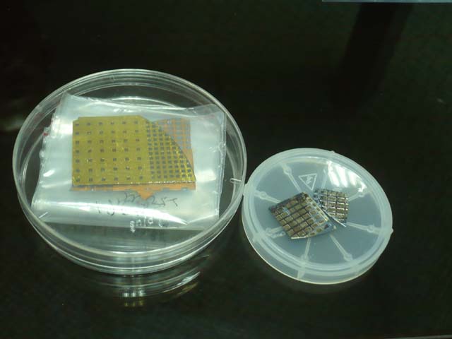
"WLP costs can be further cut with bigger wafers used," Su notes. Retrieving an experimental 4-inch WLP wafer, he says the wafer holds around 4,000 lead-frame dies. "With six-inch and even eight-inch wafer, the output can double and quadruple without changing costs," he adds. In contrast, a PPA plate can hold 144 to 288 lead frames at the most at one time, says Huang.
The WLP technology, with its obvious advantages, is an ideal solution for high-power packages for auto headlamps, streetlights and overhead projectors. Citing data from the government-backed Industrial Economics and Knowledge Center (IEK), which tracks high-tech markets worldwide, Su points out that the world WLP market is estimated to grow to US$550 million in 2010 from 2005's US$210 million, with a compound annual growth rate (CAGR) of 21%. "The rate is higher not only than the global average in the chip-making industry but also the packaging industry as a whole," he notes.
Although there are several organizations on the island, private or public, working on WLP projects, Su is the most resourceful solution provider in the rising segment, according to Huang. "The professor can handle every WLP process from epitaxy wafer-making and chip-slicing to packaging and application because he has been involved in all these segments over the past 30 years or so," he says.
Poached from Bell Lab
Su was once a Bell Lab research fellow before being poached by the Taiwan government in 1975 to develop LED technologies. He assembled metal organic chemical vapor deposition (MOCVD) chambers, the crucial equipment for making epitaxy wafers, single-handedly at a time when so such expertise existed in Taiwan. Working on a three-year contract backed by the Ministry of Economic Affairs (MOEA), Su is researching the key elements of LED lighting fixtures, covering nano materials, packaging process, thermal dissipation, driver IC, mechanical construction and illumination measurement.
Others involved in LED WLP technology on the island include the Industrial Technology Research Institute (ITRI), Solidlite Corp., VisEra Technologies Co., Ltd., Xintec Inc. and Silicon Base Development Inc. (SiDBI).
Although Taiwan already leads the world as an LED supplier by quantity, the number of its WLP providers is insignificant relative to traditional LED packagers. "I blame the shortage of WLP packagers on lack of knowledge as they all began with LED manufacturing," comments Z.M. Chen, president of SiDBI, the island's first exclusive LED WLP provider founded in 2006. "The company was set up by specialists from the silicon-chip industry to focus on the LED WLP technology," Chen says.
Optimistic
Chen is optimistic about the future of Taiwan's LED WLP industry based on the reality that Taiwan is already a world semiconductor power built on its globally-leading pure silicon foundry industry. "Taiwan has the world's leading chip-making process technologies," he stresses.
SiDBI is doing LED packaging on six-inch and eight-inch silicon wafers, with defect rates below 2%. "Our packages are available for general lighting equipment, backlight modules and auto headlights," Chen notes.
More positive proof of the feasibility of WLP packaging lies in these figures: SiDBI's packaging shows 0.75% light degradation after 1,000 hours of non-stop operation in field tests under 85C ambient temperature, which translates into 30% degradation after 40,000 hours of operation, according to Chen.


