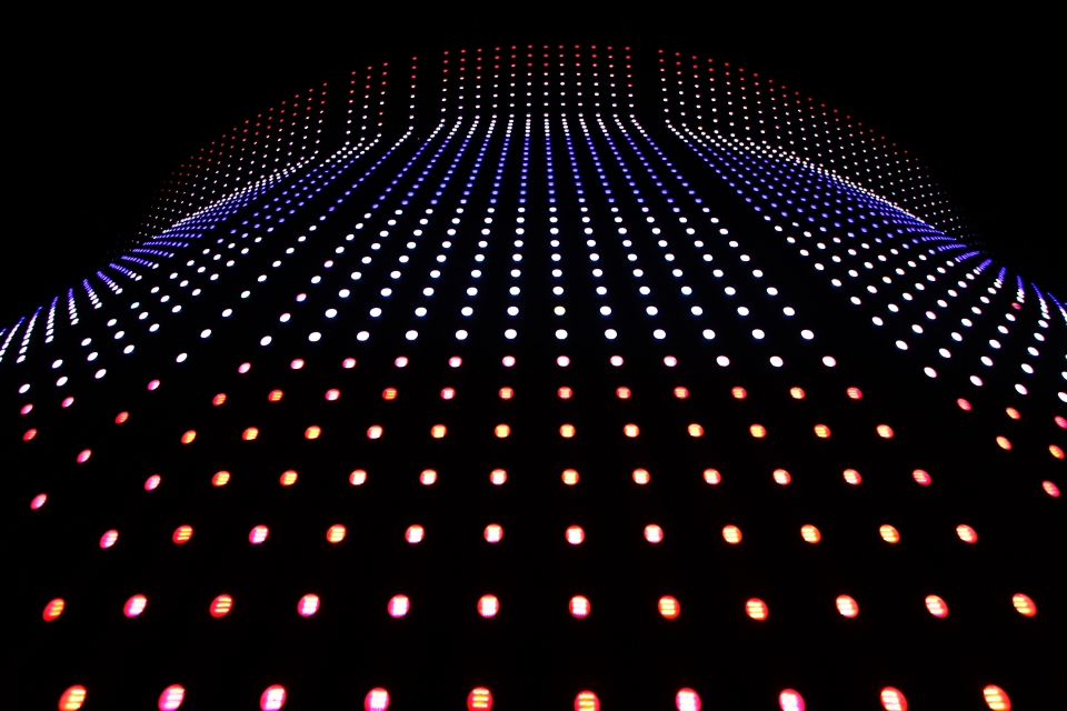
MicroLED Gains Traction as AI Drives New Applications
2026/01/27 | By Sherry ChenAs leading cloud service providers transitions from self-designed ASICs into mass production this year, the industry is also diverging from traditional GPU roadmap. Hyperscalers are accelerating the development of in-house optical communication architectures, creating a new opening for MicroLED technologies. Microsoft’s investment in MicroLED solutions, aimed at overcoming limits in data transmission, is seen as a potential inflection point that could propel Taiwanese suppliers up the value chain.
With major players such as Microsoft and TSMC committing resources, MicroLED optical interconnects are transitioning from laboratory concepts to commercial reality. For Taiwan’s LED manufacturers, the technology represents a rare opportunity to raise product value and escape the intense pricing competition of the conventional display market.
Beyond display applications, MicroLED’s high thermal tolerance makes it particularly attractive for high-speed data transmission in AI. Unlike laser solutions that are highly sensitive to heat and prone to efficiency loss and wavelength drift, MicroLEDs maintain stable performance at elevated temperatures. It addresses critical power and cooling constraints in data centers.
Equally important, the mass-transfer techniques refined in MicroLED display manufacturing provide a foundation for optical communications. High-density transfer enables multi-channel array architectures with hundreds of channels, reducing the complexity and cost associated with ultra-high-speed single-channel designs.
Analysts argue that leveraging non-display demand can accelerate large-scale MicroLED production, improve cost structures, and ultimately speed adoption in display markets. As computing competition intensifies, MicroLED is increasingly viewed as a “photonic engine” that supports AI efficiency, opening a growth pathway across display and non-display applications.